


2023.10.10
0


SHARE
Special feature : Supporting the evolution of automobiles and semiconductors Vol.4
Mitsubishi Materials Electronic Chemicals Co., Ltd.
World-class technical capabilities enable us to manufacture large crystals
With the semiconductor industry developing, the needs for materials for semiconductor manufacturing equipment are increasing. Mitsubishi Materials Electronic Chemicals, one of the Mitsubishi Materials Group companies, manufactures columnar crystal silicon. The silicon is processed into various forms, mainly as a component of semiconductor manufacturing equipment. The company is contributing to the semiconductor industry by supplying the material.
Mitsubishi Materials Electronic Chemicals is planning to increase the production of the columnar crystal silicon, aiming to produce 1.3 times as many ingots as FY2022 by 2026. By this means, the company will meet the increasing demand for materials used in semiconductor manufacturing equipment.
In recent years, there is an increasing need for reducing impurities within semiconductor manufacturing equipment. Currently, the mainstream material for semiconductors is silicon. To avoid containing impurities during the process of producing semiconductors, it is effective to use silicon, which is the common material, in the semiconductor manufacturing equipment. By using high-purity columnar crystal silicon as a component of the manufacturing equipment, the risk of containing impurities can be reduced compared to the case of using other materials, including quartz.
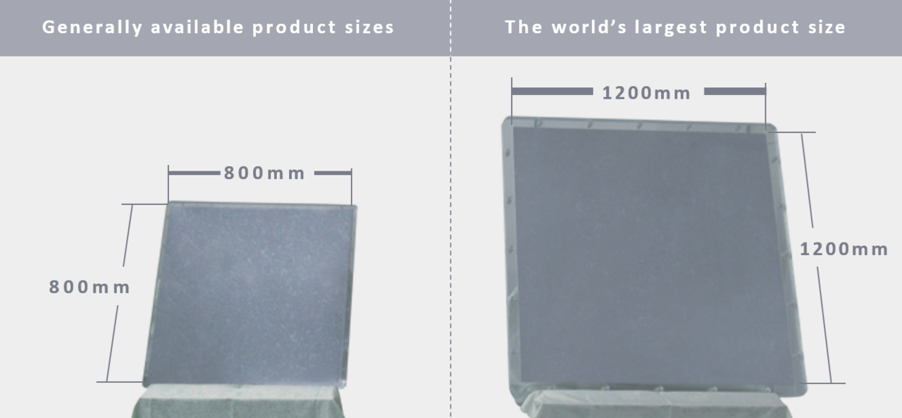
This is why columnar crystal silicon is requested for large-sized parts of semiconductor manufacturing equipment, for which other materials were conventionally used. However, large- sized silicon is easy to crack, and its manufacturing and processing requires high technical capabilities.
As such, Mitsubishi Materials Electronic Chemicals leverages its manufacturing strengths, which have been established through the high-level precision casting technology cultivated by Mitsubishi Materials. This enables the company to achieve stable production of ingots that are among the world’s largest, measuring 1200 mm in both width and length, to meet the demands of large-sized materials.
Mitsubishi Materials Group contributes to the development of the semiconductor industry by utilizing these world-class technical capabilities and establishing a system of expanded production of high value-added products.
Mitsubishi Materials Electronic Chemicals is planning to increase the production of the columnar crystal silicon, aiming to produce 1.3 times as many ingots as FY2022 by 2026. By this means, the company will meet the increasing demand for materials used in semiconductor manufacturing equipment.
In recent years, there is an increasing need for reducing impurities within semiconductor manufacturing equipment. Currently, the mainstream material for semiconductors is silicon. To avoid containing impurities during the process of producing semiconductors, it is effective to use silicon, which is the common material, in the semiconductor manufacturing equipment. By using high-purity columnar crystal silicon as a component of the manufacturing equipment, the risk of containing impurities can be reduced compared to the case of using other materials, including quartz.
This is why columnar crystal silicon is requested for large-sized parts of semiconductor manufacturing equipment, for which other materials were conventionally used. However, large- sized silicon is easy to crack, and its manufacturing and processing requires high technical capabilities.
As such, Mitsubishi Materials Electronic Chemicals leverages its manufacturing strengths, which have been established through the high-level precision casting technology cultivated by Mitsubishi Materials. This enables the company to achieve stable production of ingots that are among the world’s largest, measuring 1200 mm in both width and length, to meet the demands of large-sized materials.
Mitsubishi Materials Group contributes to the development of the semiconductor industry by utilizing these world-class technical capabilities and establishing a system of expanded production of high value-added products.
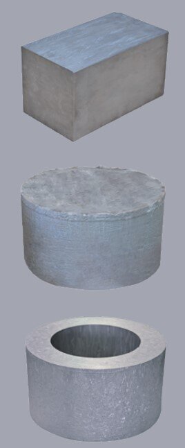
Ingots processed into various forms
What is columnar crystal silicon?
It is silicon with a crystal structure in the form of a column. To create this columnar crystal structure, crystal is grown and solidified uni- directionally, from bottom to top, when casting.
The core technology of developing columnar crystal silicon is this unidirectional solidification. This method grows crystals from the bottom, prevents volume expan- sion, and releases stress vertically to the top.
The advantage of this method is the prevention of internal cracks during solidification. The unidirectional solidification process enables the release of internal stress that occurs during solidification of the melted silicon.
Another advantage of this method is that impurities move upward and are removed by migration, increasing the purity of the silicon crystalline.
Monocrystalline silicon is mainly used in the current semiconductor manufacturing equipment market, but its physical properties restrict the flexibility of designing equipment compared to the columnar crystal silicon. In addition to providing large-sized parts, columnar crystal silicon is superior to monocrystalline silicon and other polycrystalline silicon
in bendability and machinability and can be processed into various forms, including disks, plates, and cylinders, and is thereby highly recognized.

Medium-term Management Strategy FY2031
My Challenge
My Challenge

General Manager
Silicon Parts Development Department
Silicon Parts Division Mitsubishi Materials Electronic Chemicals Co., Ltd.
Koji Tsuzukihashi
Aiming to contribute to the development of the semiconductor industry by supplying products in a timely manner
Our Silicon Parts Development Department is engaged in daily work with a focus on improving productivity. The semiconductor-elated market we are involved in is changing rapidly, so grasping the market trends, making timely capital investments, and ensuring a supply is essential to surpassing other companies. It is necessary to establish a system for producing columnar crystal silicon so that we can ensure a stable supply in line with market trends and achieve the FY2031 Strategy.
I believe that our columnar crystal silicon is the best in the world in every aspect, including quality, cost, and delivery. Our mission is to foresee a future of semiconductors and establish a system capable of meeting future demands. As a member of Mitsubishi Materials Group, we will further contribute to the development of the semiconductor industry through the production enhance- ment we have implemented.

Person in charge
Silicon Parts Manufacturing Department
Silicon Parts Division Mitsubishi Materials Electronic Chemicals Co., Ltd.
Takahiro Sasaki
Maintaining product quality to support production expansion systems
I am in charge of leading the casting site. We keep in mind to reduce losses due to human errors and ensure smooth communication at the site and aim to maintain high yields.
In silicon ingot manufacturing, temperature management of the casting furnaces is the key. The management technology for maintaining a certain temperature is required, as silicon is heated and dissolved from a solid condition and then cooled and solidified. In addition, we devise various improvements during the casting process to make silicon easy to remove from the mold. To expand production in the future, we will strive to maintain stable production and quality so that we can contribute to achieving the FY2031 Strategy.
[ Related links ]
SPECIAL FEATURE : Supporting the evolution of automobiles and semiconductors Vol.1
SPECIAL FEATURE : Supporting the evolution of automobiles and semiconductors Vol.2
SPECIAL FEATURE : Supporting the evolution of automobiles and semiconductors Vol.3
SPECIAL FEATURE : Supporting the evolution of automobiles and semiconductors Vol.5


